The Evolution of Flexible and Rigid-Flex Circuits: Key Trends Shaping the Future of PCB Technology
The world of Printed Circuit Boards (PCBs) is undergoing a major transformation, with flexible and rigid-flex circuits at the forefront of this revolution. As technology continues to push the boundaries of what is possible, these innovative circuits are enabling compact, durable, and versatile solutions for a wide range of industries. With the growing demand for miniaturized electronics, high-performance connectivity, and eco-friendly designs, flexible PCBs are quickly becoming a game-changer for electronics development.
Advanced Materials Powering the Future of Flexible PCBs
To keep up with the increasing demands of modern electronics, manufacturers are turning to advanced materials. Flexible and rigid-flex circuits are now being made from high-flexibility copper and low-permittivity dielectric materials, which improve the durability of these circuits while enhancing electrical performance, especially in high-frequency applications.
As eco-consciousness grows, there is a significant interest in using biodegradable and environmentally friendly materials. These innovations are crucial in the development of disposable electronics and wearable devices. Research is also focusing on creating materials that can withstand extreme temperatures, which is essential for industries like aerospace and automotive.
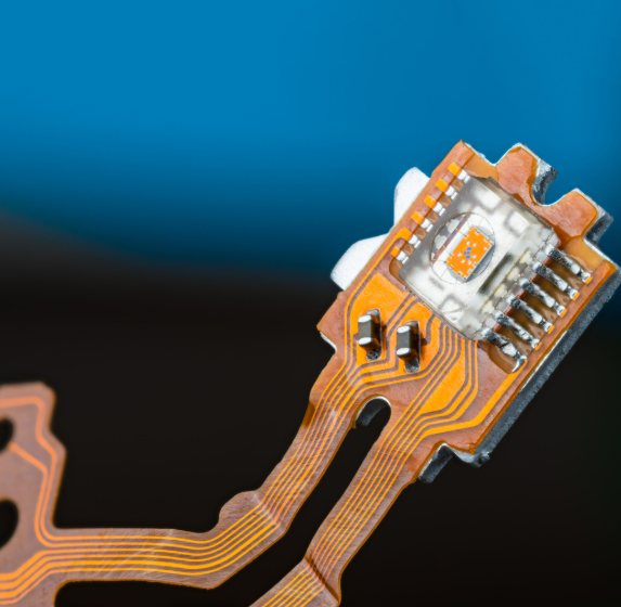
Multi-Layer Flexible Circuit Boards: The New Standard
Multi-layer flexible PCBs are making significant strides in the electronics world. These boards, which include at least three conductive layers separated by dielectric materials, combine flexibility with robust support for electronic components. Common applications include devices such as LCD displays, cameras, and digital equipment. These boards often feature high-density designs, with eight layers in LCD interfaces and six layers in digital cameras.
However, manufacturing these multi-layer flexible circuits presents several challenges. Ensuring proper alignment between layers is critical to maintaining signal integrity. Even slight misalignments can lead to significant issues, which is why precise calibration and advanced quality control methods, such as X-ray computed tomography (CT), are essential for detecting internal defects.
Additionally, high-density components generate heat, which poses a challenge for thermal management. Bending stresses can also cause delamination, so specialized materials like high-strength adhesives and cushioning layers are often used to prevent damage.
Miniaturization: Key to Advancing Flexible and Rigid-Flex Circuits
Miniaturizing flexible and rigid-flex PCBs requires advanced design techniques to reduce the space needed while still maintaining performance. Several factors come into play when achieving miniaturization:
-
Multilayer Integration: By stacking multiple layers, more components can be integrated into a single board. This eliminates the need for separate boards or additional components.
-
Reduced Trace Spacing: As the need for smaller PCBs increases, trace spacing has to be reduced. Techniques like advanced photolithography allow manufacturers to achieve trace spacing down to a few microns.
-
Thinner Dielectric Materials: Using thinner materials with lower electrical permittivity allows for even smaller and more efficient boards. This also helps minimize electromagnetic interference, which is especially important in high-density designs.
Automation and Assembly Advancements in Flexible PCBs
The automation of flexible PCB production has become a vital part of the manufacturing process. With the integration of cutting-edge technologies like 3D printing and robotic assembly lines, the production of flexible and rigid-flex PCBs has become more precise and cost-effective. Automation also allows for the customization of designs to meet specific needs, which is crucial for devices with unconventional shapes.
New assembly techniques, such as Surface Mount Technology (SMT) and wireless interconnects, enable higher reliability and efficiency in the production process. These techniques help create seamless connections and are particularly useful in reducing the mechanical complexity of flexible circuits.
Tackling 5G and IoT Challenges with Flex Circuits
The rise of 5G and IoT technologies presents unique challenges for PCB designers. As these technologies rely on higher frequencies, issues like parasitic effects, signal attenuation, and electromagnetic interference become more prevalent. Flexible and rigid-flex PCBs are particularly well-suited for these challenges, as their design allows for better control over trace thickness and insulation.
By offering optimal insulation, flexible PCBs help minimize signal loss and interference, which is critical for 5G applications and high-frequency IoT devices. These circuits enable the development of micro-antennas and signal processing modules that are both energy-efficient and interference-free.
Sustainable Manufacturing with Halogen-Free Laminates
Environmental regulations are pushing manufacturers to adopt halogen-free laminates, which replace traditional halogen-containing materials. While these eco-friendly materials are better for the environment, they come with their own set of challenges. Halogen-free laminates have different thermal and electrical properties, which can affect circuit performance, especially in high-frequency applications like IoT and 5G.
Manufacturers need to carefully select materials that balance environmental sustainability with electrical efficiency. For instance, low water absorption materials are often chosen to reduce signal loss while also complying with green standards.
Biopolymer Composites: A Greener Alternative
While epoxy resins are commonly used in PCBs, they are not the most eco-friendly option. Biopolymer composites, such as polylactic acid (PLA), offer an alternative that is more sustainable. However, biopolymers present challenges in terms of thermal stability and moisture resistance. To ensure the longevity of PCBs made from biopolymers, they often require protective coatings, especially for outdoor IoT sensors exposed to harsh weather conditions.
Low-Temperature Soldering Techniques: A Step Toward Energy Efficiency
Traditional PCB soldering processes involve high temperatures, which can increase energy consumption and negatively impact the environment. Low-temperature soldering techniques, however, minimize these issues by reducing the temperature needed during the soldering process. This not only saves energy but also prevents damage to sensitive materials like biopolymers.
For IoT and 5G applications, low-temperature soldering is particularly beneficial, as it helps avoid thermal expansion damage and enhances the overall quality of the final product.
Overcoming Challenges in Flexible PCB Production
While flexible and rigid-flex PCBs offer numerous advantages, their production is not without challenges:
-
High Production Costs: The complexity of flexible circuit design and the use of advanced materials increase production costs. Multilayer layouts, thin materials, and additional processes like copper plating and protective layers all contribute to higher expenses.
-
Design Complexity: Managing trace geometry and selecting the right materials is crucial for ensuring that flexible PCBs are durable and functional. Designers need to carefully balance flexibility with the need for robust connections and stress resistance.
-
Heat Management: Materials used in flexible circuits typically have lower thermal conductivity, making it difficult to manage heat dissipation. Solutions like metallized traces and insulation layers are used to address these challenges.
-
Testing and Quality Control: Flexible PCBs require advanced testing techniques due to their complex structures. Standard testing methods like Automated Optical Inspection (AOI) may not be sufficient. More advanced techniques, like X-ray microscopy, are needed to detect microcracks or dielectric breakdowns.
-
Integration and Durability: Flexible PCBs are often used in devices exposed to constant bending, twisting, or vibrations. To ensure durability, designers apply reinforcement at key stress points and manage trace geometry to prevent damage during use.
Conclusion
Flexible and rigid-flex PCBs are transforming the electronics industry, enabling the development of lighter, more durable, and compact devices. However, challenges remain in terms of production costs, material selection, and testing. By embracing advanced materials, automation, and new assembly techniques, manufacturers are paving the way for more efficient and environmentally friendly PCB solutions. As the demand for high-frequency applications like 5G and IoT continues to rise, flexible circuits will play an increasingly important role in shaping the future of electronics.